NanoOptics Team
Quantum Optics and Quantum Information at the nanoscaleTEAM MEMBERS
PERMANENT STAFF
- Quentin Glorieux
- Alberto Bramati
- Elisabeth Giacobino
POSTDOC
- Rajiv Bodeda
PHD STUDENT
- Maxime Joos
- Chiengjie Ding
- Stefano Pierini
Why NanoOptics ?
Quantum electrodynamics (QED) 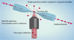 is a major research topic in modern Physics dealing with the coupling of a single emitter to a mode of the electromagnetic field. Today, it is possible to build a system where the fundamental properties of a single emitter are dramatically modified by this coupling. Various emitters have been studied from individual atoms or ions to solid states systems as epitaxial quantum dots or semiconductor nanocrystals. Applications range from secure communication and random number generation to biological imaging. Fundamental tests of quantum theory are also of concern, with the possibility to study strong light–matter interaction.
In order for quantum communication to become realistic with an implementation at a large scale, it is absolutely critical to be able to miniaturize the elements that will be parts of the future networks. In optics, miniaturization of photonics devices, widely called nanophotonics, is a very active research topic.
During the last decade, multiple Nano-optics and nanophotonics devices that outperform their traditional counterparts (faster operations, lower energy consumption…) have been demonstrated.
The new challenging task that we are now facing is to couple different devices at a nanometric scale in order to surpass their individual properties. These hybrid systems will then allow us to observe new physics effects and to develop innovative devices.
In the NanoOptics Team, we investigate original approaches for coupling optical fibers or more generally waveguides to various solid-state quantum emitters (semiconductor nanocrystals, nanodiamonds…).
The NanoOptics Team works on 3 main project :
-
Q-crystals : Quantum Optics with high-quality semiconductor nanocrystals
-
COSINE : Nanophotonics structures with optical nanofibers
-
Nano² : Quantum nano-emitters coupled to nanofibers
Research project : Q-crystals
Quantum Optics with high-quality semiconductor nanocrystalsRecent publications
-
M. Manceau, S. Vezzoli, Q. Glorieux, E. Giacobino L. Carbone, M. De Vittorio J- P. Hermier, A. Bramati. CdSe/CdS dot–in–rods nanocrystals fast blinking dynamics. ChemPhysChem, 19, 1. (2018).
- S. Vezzoli, M. Manceau, G. Lemenager, Q. Glorieux, E. Giacobino, L. Carbone, M. De Vittorio and A. Bramati, Exciton fine structure of CdSe/CdS nanocrystals determined by polarization microscopy at room temperature. ACS Nano, 9, 7992 (2015)
-
M. Manceau, S. Vezzoli, Q. Glorieux, F. Pisanello, E. Giacobino, L. Carbone, M. De Vittorio and A. Bramati, Effect of charging on CdSe/CdS dots-in-rods single-photon emission. Phys. Rev. B, 90, 035311 (2014)
Optical characterization of room temperature single photon sources
We work primarily with II-VI semiconductor nanocrystals. 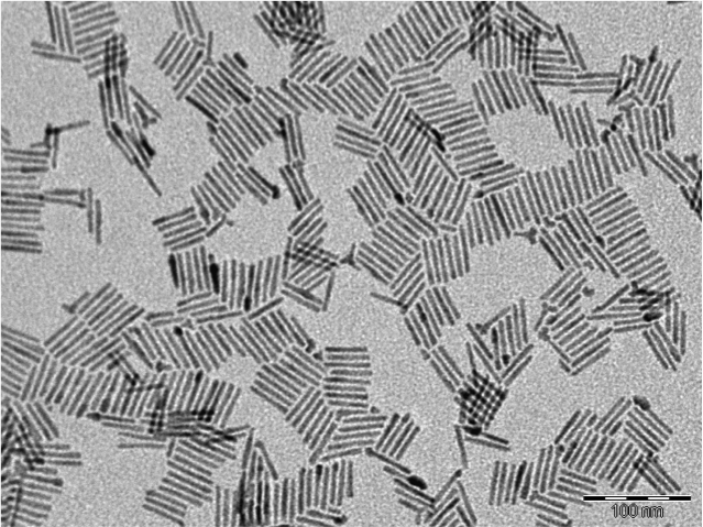 These quantum dots can emit light at room temperature and are synthesized via wet chemistry.
They are highly interesting sources of single photon under continuous wave or pulse excitation and at room temperature. Their typical structure is a spherical core of CdSe with a diameter between 3 and 10 nm embedded in a CdS shell. The shell shape can be of two types : spherical (quantum dots) or elongated (dot–in–rods). A problem with commercially available quantum dots is the blinking : period of time with zero emission. Thanks to an ongoing collaboration with a research group in nanocrystal synthesis (Pr. Carbone Group at NNL in Lecce), we are working with high quality dot–in–rods with near complete suppression of blinking at ambient temperature. The suppression of blinking was a major technological challenge that is now well controlled by our collaborators and that opens the way to quantum information experiments with semiconductor nanocrystals.
Narrowing the linewidth of semiconductor nanocrystals
To date, single photons emitted by nanocrystals usually have a large linewidth (several nm) at room temperature, with inhomogeneous broadening and a time drift of the emitted frequencies (spectral diffusion). We investigate various approaches for narrowing the linewidth of these emitters.
- Cryogenic operation. A straightforward path to narrow linewidths with solid-state emitters is to go to cryogenic temperature. Narrow lines have been obtained at 2K with excitation on the zero-phonon lines of the lowest levels, but with photoluminescence detection at a different wavelength. This solution have the advantage of the tunability of the linewidth with respect to the temperature, and is of great interest for detailed investigation in a laboratory environment. However for future applications, room temperature experiments should also be developed.
- Resonant excitation. A second approach for narrowing the linewidth is to take advantage of the Heitler effect. Indeed, unlike the spontaneously emitted photons, the elastically scattered photons in the Heitler regime are phase-locked to the excitation laser with ideally infinite mutual coherence, accentuating their potential for quantum interference. Resonant scattering with a weak excitation has been demonstrated to allow indistinguishable photons in the case of self-assembled quantum dots at cryogenic temperature and is believed to work similarly at room temperature with nanocrystals. Resonant excitation will become possible thanks to high spatial rejection of the excitation beam with the nanofiber configuration.
Research project - COSINE
Nanophotonics structures with optical nanofibersRecent Publications
- W. Geng, M. Manceau, N. Rahbany, V. Sallet, M. De Vittorio, L. Carbone, Q. Glorieux, A. Bramati, C. Couteau, Localised excitation of a single photon source by a nanowaveguide. Scientific Reports, 6, 19721 (2016).
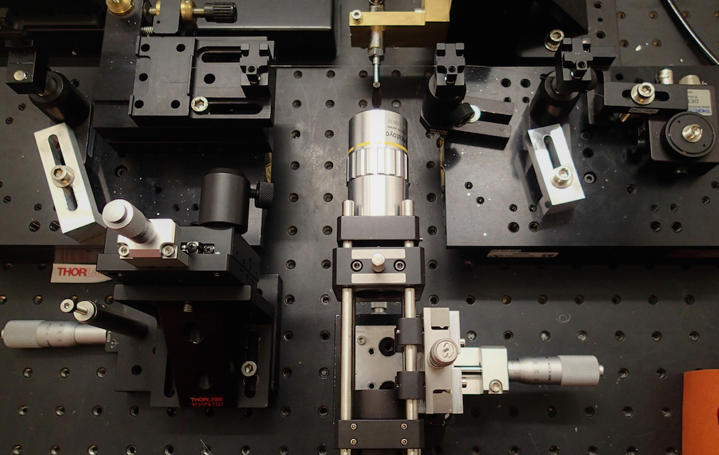
Nano-waveguide fabrication with tapered fiber
 One of the most commonly faced problem with semiconductor single photon sources is to implement fluorescence collection with high efficiency. For this purpose many ideas have been proposed and one of the key point is to achieve strong confinement of the field using photonic or plasmonic nanostructures.
Tapered optical nanofiber
There have been spectacular recent successes in this field brought by the merging of nanofiber optical cavity systems with cold neutral atoms. For example, it has been demonstrated that 28% of a single atom fluorescence can be channeled into the guided mode of a sub-wavelength tapered optical nano-fibers (TONF).
We have build a tapering bench based on commercial optical fibers elongated and tapered to 300 nm diameter.
Careful SEM characterizations have demonstrated a good agreement with our simulated pulling profile.
Photonic resonators with nanofibers
Optical cavities are often employed to increase the interaction between light and matter. A natural step forward for nanofiber-based hybrid systems is therefore the use of a cavity that can substantially enhance the coupling of the nano-emitter emission into the nanofiber. Indeed the interaction is enhanced by the transverse confinement of the field in the fiber core as well as the longitudinal confinement of the field between the mirrors. It has been theoretically predicted that the channeling collection efficiency into the nanofiber guided modes can be enhanced to 94% by incorporating a moderate finesse cavity structure to the nanofiber.
Fabry-Perot nanofiber cavities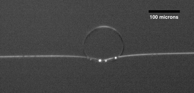
Recently, various nano-fabrication technologies have been successfully applied to micro/nano-size optical- fibers to create fiber Bragg gratings (FBG) : excimer laser index modification, femtosecond laser ablation, and ion beam milling. Contrary to ion beam milling that requires nanofabrication capabilities, the laser techniques can be implemented directly in an optics laboratory as the LKB. The technique selected for optical writing is based on an excimer laser as it is flexible (grating steps can be adjusted easily) and directly possible to implement in our laboratory with a comparatively limited cost. It has been demonstrated that, with careful control of the grating writing process and good choice of the glass material, a FBG cavity can have a finesse greater than 1000 and a linewidth of a few MHz.
Toroidal resonator with nanofibers
An alternative approach without permanent modification of the fiber structure will also be investigated. This technique relies on a resonator based on a knot of the TONF. By carefully manipulating a TONF, it is possible to realize knots as small as 50 μm in diameter, with an associated free spectral range of 14 nm. Numerical simulations conducted in the LKB group have predicted a finesse of 100 with realistic nanofiber parameters.
Hybrid photonic-plasmonic nanostructures.
In order to strengthen the coupling between the emitters and a tapered optical nanofiber, we are investigating the effect of plasmonic enhancement. The presence of a plasmonic structure at the surface of the nanofiber can result in an increase of the local density of optical states (LDOS) and therefore in an increase of the probability of coupling between the emitter and the dielectric structure. However, due to Ohmic losses, the propagation length of a surface plasmon is much smaller than the propagation length of photons inside an optical fiber. 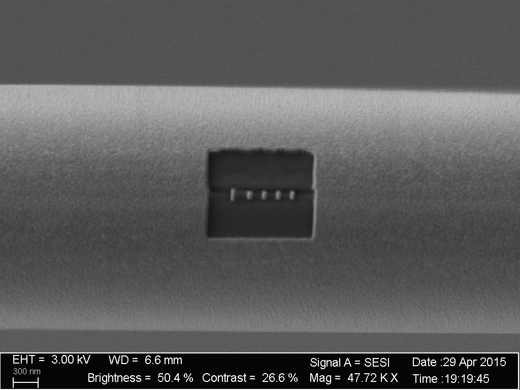
Therefore, in order to keep the advantages of both dielectric and plasmonic environments, it will be interesting to limit the plasmon-emitter interaction region to a small size, devoted to the enhancement of the decay rate of the emitter into the guided mode while using the guided mode into the fiber as long range energy transfer vector. We are working to design and optimise these nanostructures by numerical simulations using commercial FDTD softwares.
Structures under study are plasmonic nanoantennas (see image of a Gold Yagi-Uda antenna grown by M. Mivelle on a nanofiber ) and plasmonic gratings. Hot spots of the hybrid mode present in the proximity of the plasmonic structures should ensure a coupling of the fluorescence of emitters with the nanostructure. The use of the fluorescent scanning probe will allow us to position precisely the emitter in correspondence with the hot-spot in order to maximise the coupling of the fluorescence photons into the guided mode and vice-versa.
Research project - Nano²
Quantum nano-emitters coupled to nanofibers- M. Joos, C. Ding, V. Loo, G. Blanquer, E. Giacobino, A. Bramati, V. Krachmalnicoff, Q. Glorieux. Polarization Control of Linear Dipole Radiation Using an Optical Nanofiber. Physical Review Applied, 9, 064035 (2018).
Recently we have developed a technique to study the coupling of high quality non-blinking CdSe-CdS nanorods with tapered optical nanofiber (TONF). The high collection efficiency of the TONF method associated with the advantages of dot-in-rods nanocrystal (room temperature fluorescence, non-blinking, polarization control) are key ingredients to realize a high quality single photon source.
The main objective of this experiment is to investigate original approaches for coupling optical fibers to solid-state quantum emitters (semiconductor nanocrystals).
Method :
A CdSe-CdS nanorod is deposited on the fiber using a nano- positionning system with a lateral precision of 0.1 μm. An excitation laser (cw or pulsed laser diode) is then focused using an inverted microscope on the nanorod, and fluorescence emission is collected at both side of the fiber and measured with avalanche photodiodes. The detection setup can be modified to measure the g(2) correlation function and verify that the nanorod is indeed a single quantum emitter.

- Nanocrystal deposition on a nanofiber
Preliminary results
Preliminary results (light collection through the fiber, g(2) measurements) have been obtained recently and we have managed to produce a TONF with a waist of 300 nm and a transmission greater than 98%.
Moreover, direct photoluminescence signal collected through the nanofiber after excitation in free space at 405 nm, with up to 23% efficiency. With various upgrades we are currently implementing, this device is expected to be the first room temperature single photon source with collection efficiency near unity.
Deterministic coupling of a single quantum emitter in nanophotonic structures
For most of our application, we will need to have nanometric resolution on the deposition of the quantum emitters in our photonic nanostructure. To do so we are using a fluorescent scanning nanoprobe developed at Institut Langevin in the group of Yannick De Wilde and Valentina Krachmalnicoff. With this technique it is possible to graft fluorescent objects sized between 20 to 100 nm on the apex of the AFM tip (tapered silica fiber).
Method
The established grafting procedure is the following:
- first, the emitters are spread on a glass cover-slide, in order to reach an average distance of about 10 μm between two close by emitters;
- second, the AFM tip is approached to the surface;
- third, the AFM tip scans the region where the emitter to be grafted is located. When the extremity of the AFM tip coincides exactly with the position of the emitter, the emitter stays stuck to the tip. The fluorescent tip is then retracted and moved on the sample of interest.
During each stage of this procedure the tip and the emitter are monitored by using an EMCCD camera which registers the fluorescence signal in wide field. The signature of the success of the procedure is the disappearing of the grafted emitter from the field of view of the camera when the AFM tip is lifted by a few microns on the top of the glass cover slide. Adhesion between the emitter and the tip is so good that the emitter can remain grafted on the tip for several hours. As the grafting procedure is very well mastered, we believe that it will be possible to have a perfect control of the complementary procedure allowing to release the emitter on the sample in a deterministic way. A thorough study of the orientation of the dipole moment of the emitter when it is grafted on the tip and when it is deposited on the sample will be done.
How to attach a nano-emitter to a AFM tip ?
Credit : Valentina Krachmalnicoff (Institut Langevin)
Emitter release
Finally, different strategies can be used to release the emitter on the TONF. One possibility will be to strongly shake the tip by increasing the oscillation amplitude of the tuning fork. This technique will work but it will probably not be the most precise. A second possibility will be to approach the fluorescent AFM tip to the sample and to push it against the substrate in order to increase the adhesion between the sample and the emitter. Following the same idea, we shall try to scratch the functionalized tip on the sample until the emitter is wiped away.
Non-resonant cavity-QED
Towards strong coupling
Thanks to these various resonators we are developing, we plan to study the strong coupling between a cavity and a semiconductor nanocrystal. Placing a single emitter within a high finesse cavity have been demonstrated in various systems from single atoms to epitaxial quantum dots or nanocrystals. Our structure is a quite different system, as nanocrystal are single photon sources from cryogenic to room-temperature. Therefore, the linewidth of the emitter can be tuned by changing the temperature and different regimes can be investigated. For example the regime of a narrow cavity coupled to a relatively broad emitter will be investigated.
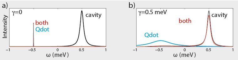
Non-resonant cavity-QED
Non-resonant cavity-QED has been predicted theoretically by Auffeves et al. A promising application of this effect is the cavity feeding (or cavity pulling). In this regime, the weak coupling between a spectrally large emitter and a detuned narrow cavity dramatically modifies the emitter properties . The linewidth and the wavelength of the emitter will change to match the linewidth and the resonance frequency of the cavity. The origin of this effect is believed to be the pure dephasing term coming from the phonon-exciton coupling. This coupling is directly linked to the temperature and therefore we can directly study the role on non-resonant cavity-QED. This setup is therefore a great test bench to study cavity-QED with one more degree of freedom that can be adjusted by controlling the temperature, not accessible with the single atom or epitaxial quantum dots counterparts. On a more technological side, this is an alternative approach to control the linewidth of the single photon emitted by a single nanocrystal